Various stages of ASIC/FPGA
 Specification :
This is the stage at which we define what are the important parameters of the system/design that you are planning to design. A simple example would be: I want to design a counter; it should be 4 bit wide, should have synchronous reset, with active high enable; when reset is active, counter output should go to "0".
High Level Design:
This is the stage at which you define various blocks in the design and how they communicate. Let's assume that we need to design a microprocessor: high level design means splitting the design into blocks based on their function; in our case the blocks are registers, ALU, Instruction Decode, Memory Interface, etc
 Micro Design/Low level design:
Low level design or Micro design is the phase in which the designer describes how each block is implemented. It contains details of State machines, counters, Mux, decoders, internal registers. It is always a good idea to draw waveforms at various interfaces. This is the phase where one spends lot of time.
 RTL Coding:
In RTL coding, Micro design is converted into Verilog/VHDL code, using synthesizable constructs of the language. Normally we like to lint the code, before starting verification or synthesis.
Simulation :
Simulation is the process of verifying the functional characteristics of models at any level of abstraction. We use simulators to simulate the Hardware models. To test if the RTL code meets the functional requirements of the specification, we must see if all the RTL blocks are functionally correct. To achieve this we need to write a testbench, which generates clk, reset and the required test vectors. A sample testbench for a counter is shown below. Normally we spend 60-70% of time in design verification.
We use the waveform output from the simulator to see if the DUT (Device Under Test) is functionally correct. Most of the simulators come with a waveform viewer. As design becomes complex, we write self checking testbench, where testbench applies the test vector, then compares the output of DUT with expected values.

There is another kind of simulation, called
timing simulation, which is done after synthesis or after P&R (Place and Route). Here we include the gate delays and wire delays and see if DUT works at rated clock speed. This is also called as
SDF simulation or
gate level simulation.
Synthesis :
Synthesis is the process in which synthesis tools like design compiler or Synplify take RTL in Verilog or VHDL, target technology, and constrains as input and maps the RTL to target technology primitives. Synthesis tool, after mapping the RTL to gates, also do the minimal amount of timing analysis to see if the mapped design is meeting the timing requirements
 Place & Route

 Post Si Validation
Once the chip (silicon) is back from fab, it needs to be put in a real environment and tested before it can be released into Market. Since the simulation speed (number of clocks per second) with RTL is very slow, there is always the possibility to find a bug in Post silicon validation
---------------------------------
0.可合成的
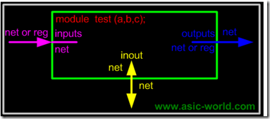
/* module
|----------------------- |
net/reg | |
=======> |net net/reg |===>net
input | | outport
port | /\ |
| ||net |
|-----------------------|
||net
\/inout port
synthesis verilog:
include;;define;module'endmodule;parameter;input'output'inout;wire'wand'wor
reg;begin'end;always;assign;@'posedge'negedge;for;if'else;case'casex'casez;
function;task;defparam'#;?:;{{}};{}
binary bit-wise operators
~;&;|;^;~^;
logical operators:
!;&&;||
2's complement:
|;-;*
relational operators:
>;<;>=;<=
equality operators:
==;!=
logical shift operatos:
>>;<<
*/
1.data type(drive)
reg ,wire;
reg和wire的主要區別是,reg類型的訊號只能在過程塊(後面會談到)中賦值,而wire類型的訊號只能在過程塊外賦值。這兩種訊號類型都可以出現在過程塊內部和外部的賦值運算符右邊。
使用關鍵字reg並不一定意味著編譯器會製作一個暫存器,理解這一點是非常重要的。清單2的程式碼中有一個reg類型8位元寬的內部訊號out。該模組使用暫存器源於always模組(過程塊的一種)的編程方式。值得注意的是,訊號a是一個wire類型,因此只能在連續賦值(continuous assignment)語句中賦值,而reg類型的out訊號只能在always塊中賦值。
2.variable assignment
在verilog 中
組合邏輯combinational logic,有二個方法來model
使用assign 及always statement
循序邏輯sequential logic,只有一個model
只能用always statement
而在initial statement中,只能用在test bench而已
3.
always block
always block should have a sensitive list or a delay associated with it.
There are two types of sensitive list: level sensitive (for combinational circuits) and edge sensitive (for flip-flops).
level sensitive:即指說是由組合邏輯產生的H,L
edge sensitive:則是由flip-flops,邊緣
在always中,it can not drive wire data type, but can drive reg and integer data types.
always  @ (a or b or sel)
begin
  y = 0;
  if (sel == 0) begin
    y = a;
  end else begin
    y = b;
  end
end
always  @ (posedge clk )
if (reset == 0) begin
  y <= 0;
end else if (sel == 0) begin
  y <= a;
end else begin
  y <= b;
end
We can have an always block without sensitive list, in this case we need to have a delay as shown in the code below.
always  begin
  #5 clk = ~clk;
end
4.
Assign Statement
only combinational logic and it is executed continuously.
5.funcion and task
Functions and tasks have the same syntax; one difference is that
tasks can have delays, whereas functions can not have any delay. This means that
function can be used for modeling combinational logic.
組合邏輯不會有delay的。

A second difference is that
functions can return a value, whereas tasks can not.
6.
Numbers in Verilog
- Sized or unsized numbers (Unsized size is 32 bits)
- In a radix of binary, octal, decimal, or hexadecimal
- Radix and hex digits (a,b,c,d,e,f) are case insensitive
- Spaces are allowed between the size, radix and value
Syntax: <size>'<radix><value>;
- When <size> is smaller than <value>, then leftmost bits of <value> are truncated
- When <size> is larger than <value>, then leftmost bits are filled, based on the value of the leftmost bit in <value>.
- Leftmost '0' or '1' are filled with '0'
- Leftmost 'Z' are filled with 'Z'
- Leftmost 'X' are filled with 'X'
 Real Numbers
- Verilog supports real constants and variables
- Verilog converts real numbers to integers by rounding
- Real Numbers can not contain 'Z' and 'X'
- Real numbers may be specified in either decimal or scientific notation
- < value >.< value >
- < mantissa >E< exponent >
- Real numbers are rounded off to the nearest integer when assigning to an integer.
 Signed and Unsigned Numbers
Any number that does not have negative sign prefix is a positive number. Or indirect way would be "Unsigned".
minus sign before the size for a constant number, thus they become signed numbers.(2's complement)

7.
Modules
- Modules are the building blocks of Verilog designs
- You create the design hierarchy by instantiating modules in other modules.
- You instance a module when you use that module in another, higher-level modul
 Ports
Ports
- Ports allow communication between a module and its environment.
- All but the top-level modules in a hierarchy have ports.
- Ports can be associated by order or by name.
  1: module addbit (
  2: a      , // first input
  3: b      , // Second input
  4: ci     , // Carry input
  5: sum    , // sum output
  6: co       // carry output
  7: );
  8: //Input declaration
  9: input a;
 10: input b;
 11: input ci;
 12: //Ouput declaration
 13: output sum;
 14: output co;
 15: //Port Data types
 16: wire  a;
 17: wire  b;
 18: wire  ci;
 19: wire  sum;
 20: wire  co;
 21: //Code starts here
 22: assign {co,sum} = a + b + ci;
 23:
 24: endmodule // End of Module addbit
  1: //-----------------------------------------------------
  2: // This is simple adder Program
  3: // Design Name : adder_explicit
  4: // File Name   : adder_explicit.v
  5: // Function    : Here the name should match
  6: // with the leaf module, the order is not important.
  7: // Coder       : Deepak Kumar Tala
  8: //-----------------------------------------------------
  9: module adder_explicit (
 10: result        , // Output of the adder
 11: carry         , // Carry output of adder
 12: r1            , // first input
 13: r2            , // second input
 14: ci              // carry input
 15: );
 16:
 17: // Input Port Declarations
 18: input    [3:0]   r1         ;
 19: input    [3:0]   r2         ;
 20: input            ci         ;
 21:
 22: // Output Port Declarations
 23: output   [3:0]  result      ;
 24: output          carry       ;
 25:
 26: // Port Wires
 27: wire     [3:0]    r1        ;
 28: wire     [3:0]    r2        ;
 29: wire              ci        ;
 30: wire     [3:0]    result    ;
 31: wire              carry     ;
 32:
 33: // Internal variables
 34: wire              c1        ;
 35: wire              c2        ;
 36: wire              c3        ;
 37:
 38: // Code Starts Here
 39: addbit u0 (
 40: .a           (r1[0])        ,
 41: .b           (r2[0])        ,
 42: .ci          (ci)           ,
 43: .sum         (result[0])    ,
 44: .co          (c1)
 45: );
 46:
 47: addbit u1 (
 48: .a           (r1[1])        ,
 49: .b           (r2[1])        ,
 50: .ci          (c1)           ,
 51: .sum         (result[1])    ,
 52: .co          (c2)
 53: );
 54:
 55: addbit u2 (
 56: .a           (r1[2])        ,
 57: .b           (r2[2])        ,
 58: .ci          (c2)           ,
 59: .sum         (result[2])    ,
 60: .co          (c3)
 61: );
 62:
 63: addbit u3 (
 64: .a           (r1[3])        ,
 65: .b           (r2[3])        ,
 66: .ci          (c3)           ,
 67: .sum         (result[3])    ,
 68: .co          (carry)
 69: );
 70:
 71: endmodule // End Of Module adder
Port Connection Rules

- Inputs : internally must always be of type net, externally the inputs can be connected to a variable of type reg or net.
- Outputs : internally can be of type net or reg, externally the outputs must be connected to a variable of type net.
- Inouts : internally or externally must always be type net, can only be connected to a variable net type.
- Width matching : It is legal to connect internal and external ports of different sizes. But beware, synthesis tools could report problems.
- Unconnected ports : unconnected ports are allowed by using a ",".
- The net data types are used to connect structure.
- A net data type is required if a signal can be driven a structural connection.
  1: module explicit();
  2: reg clk,d,rst,pre;
  3: wire q;
  4:
  5: // Here q_bar is not connected
  6: // We can connect ports in any order
  7: dff u0 (
  8: .q   (q),
  9: .d  (d),
 10: .clk  (clk),
 11: .q_bar  (),
 12: .rst  (rst),
 13: .pre  (pre)
 14: );
 15:
 16: endmodule
 17:
 18: // D fli-flop
 19: module dff (q, q_bar, clk, d, rst, pre);
 20: input clk, d, rst, pre;
 21: output q, q_bar;
 22: reg q;
 23:
 24: assign q_bar = ~q;
 25:
 26: always @ (posedge clk)
 27: if (rst == 1'b1) begin
 28:   q <= 0;
 29: end else if (pre == 1'b1) begin
 30:   q <= 1;
 31: end else begin
 32:   q <= d;
 33: end
 34:
 35: endmodule
Flip-flop (electronics)
http://en.wikipedia.org/wiki/Flip-flop_(electronics)
http://opencores.org/project,gpiohttp://www.fpga4fun.com/MusicBox1.htmlhttp://www.knjn.com/FPGA-FX2.htmlhttp://www.public.tw/prog/lock/subsite/front/Index01_Content.aspx?sid=12&aid=A&tid=3&nid=18&cid=181http://www.asic-world.com/verilog/syntax2.htmlhttp://www.rose-hulman.edu/~doering/PLD_Oasis/verilog_examples.htm


